AUO’s Sustainability Initiatives Shapes Alternative Product Development; Driving For Efficiency
By Dave Haynes

Sustainability has long been a central corporate initiative for AUO, and the company even appointed a Chief Sustainability Officer back in 2018, well before many competitors started sharing their “green” initiatives.
AUO has an R&D mindset of looking for ways to reduce power consumption of products, the carbon footprint and manufacturing and packaging waste. Kevin Guo of AUO Display Plus says AUO has initiated these efforts, but it increasingly hears sustainability questions and expectations from customers.
“They’ll push this now, not only power reduction, but also recycling material. They give us a target, and when it needs to be achieved,” says Guo.
That has taken AUO’s R&D teams down a couple of similar but different paths, working on displays that consume far less power than conventional products.
Cholesteric LCDs
Cholesteric liquid-crystal displays, or ChLCDs for short, use a special liquid crystal material that reflects light, instead of generating it. In broad terms, these are reflective displays that, like e-paper, use the available ambient light to show information.
They are bistable, meaning they can show a static image indefinitely, without continuously drawing power. They’re also easier on eyes, with no glare and none of the harsh blue light the backlighting arrays that drive conventional flat panel displays.
AUO is targeting two primary markets for ChLCD deployment: outdoor displays and transportation. The technology offers significant advantages for outdoor use. Along with ultra-low power consumption and image retention without power, these displays have a wide temperature tolerance, and good color performance.
For transportation applications, the displays are specifically designed to handle extreme cold and meet rigorous railway vibration standards, making them suitable for in-vehicle information systems.
Color E-Paper
AUO’s head office is just a short walk down a street from the head office of e-paper giant E Ink, and the two companies are collaborating on developing large-format color e-paper displays that could take the place of posters for retail and digital out of home advertising.
E Ink will provide color modules while AUO will offer integrated software and hardware technologies, along with the thin film transistor backplane components. The vivid, high-saturation colours and print-like look of E Ink’s Spectra 6 best align with the demands of brands.
As with ChLCD technology, color e-paper is reflective and bi-stable – only needing power when images are refreshed on screens. Displays can run for months off a small battery, and can be recharged using collector arrays, whether the light is from the sun or even manmade light.
Large-size color e-paper displays represent a transformative technology for the retail sector, enhancing how messages are delivered to customers while streamlining inventory management. By facilitating timely and accurate communication, these displays help retailers reduce product inventory and optimize remote management processes. This efficiency not only allows retailers to react swiftly to market demands but also paves the way for significant cost savings.
Furthermore, these advancements can translate into tangible benefits for end customers, who are likely to enjoy more frequent discounts on products offered at competitive prices. “In essence, Large-size color ePaper displays cultivate a win-win-win scenario, benefiting suppliers, retailers, and consumers.” says SI Cheng, GM of AUO’s smart retail business group. “As retailers leverage this innovative solution, they become better equipped to meet customer needs, thereby driving sales and improving overall satisfaction.”
Under the leadership of SI Cheng, the potential for Large-size color e-paper displays to revolutionize the retail experience becomes increasingly evident, enabling all parties involved to thrive in a dynamic marketplace.
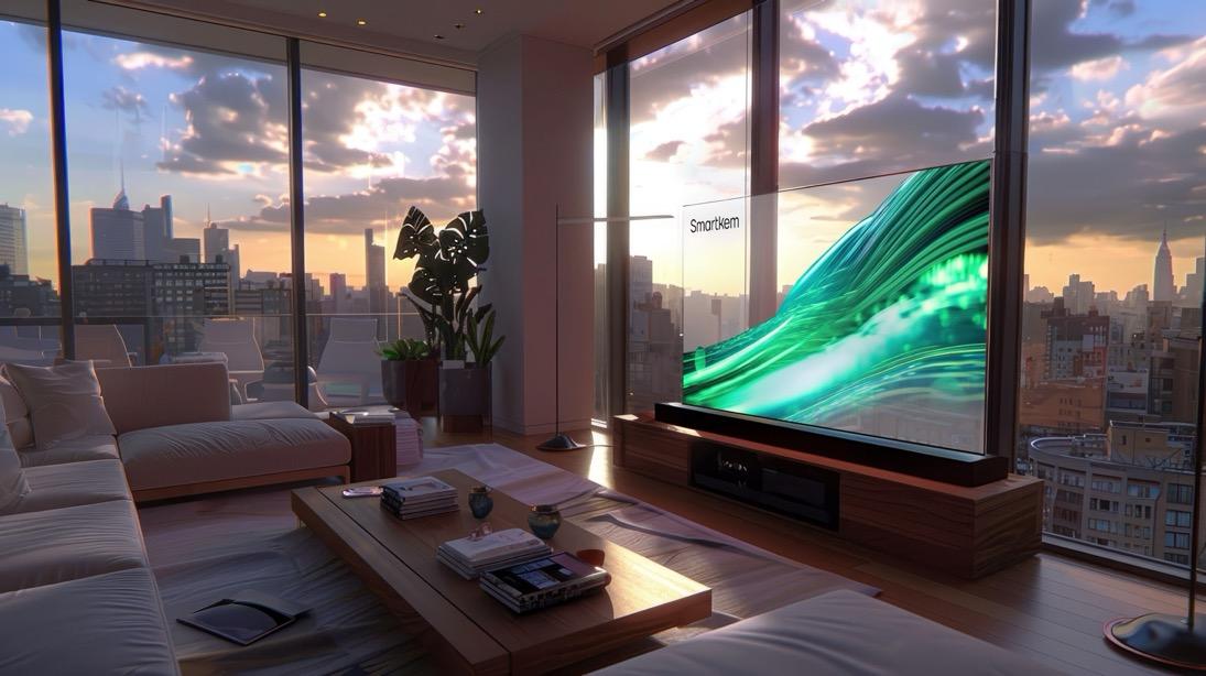
Smartkem, a Manchester-based chemical technology company, has announced a partnership with Taiwan’s AU Optronics (AUO) to develop a new approach to microLED display manufacturing that has the potential, at least, to address the primary barrier in microLED adoption: manufacturing costs.
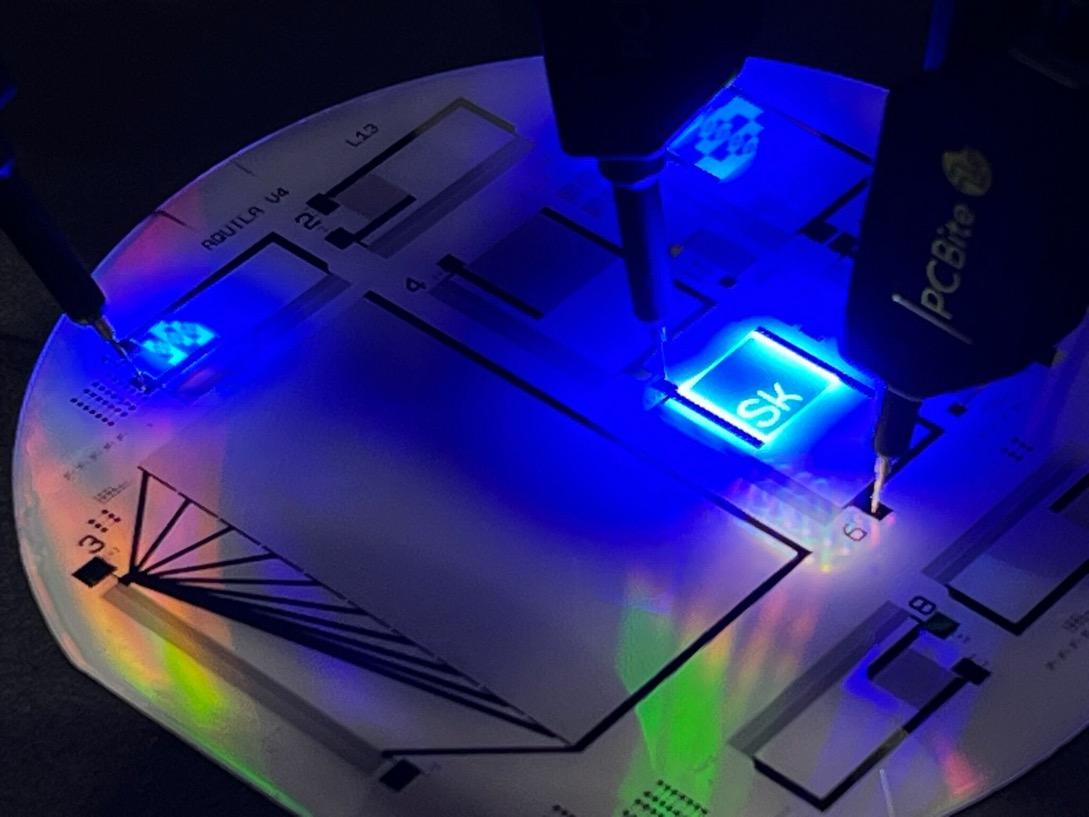
The partnership centers on Smartkem’s organic thin-film transistor (OTFT) technology, which uses semiconductor and dielectric inks applied directly to display substrates. This process operates at lower temperatures than conventional methods and uses plastic substrates instead of the more common glass.
Current microLED displays sell at premium prices, with Samsung’s 89-inch model manufactured by AUO priced at $110,000. That high cost reflects complex manufacturing processes, including precise LED placement and laser welding requirements.
Smartkem’s approach is very different. The company’s liquid electronic polymers are applied through a pouring process, potentially eliminating several costly manufacturing steps. The technology enables direct application of transistors onto microLEDs, bypassing traditional mass transfer and laser welding processes.
The initial development focuses on creating a transparent, rollable microLED display. While that visual bling of a flexible, roll-up, roll-down screen may generate attention, the technology’s potential to lower manufacturing costs is arguably much more significant.
Ian Jenks, Smartkem’s Chairman and CEO, explains the economic implications: “Our transistor technology is expected to enable efficient microLED display production at commercially viable costs. The potential exists to reduce prices from current levels of $100,000 to mass market price points.”
MicroLED display adoption faces two primary challenges: production costs and yield rates. Current manufacturing processes require precise placement of millions of microscopic LEDs, with necessarily-tight quality control requirements.
This technology effort has several potential manufacturing advantages:
1. Lower processing temperatures, enabling direct transistor application;
2. Elimination of complex mass transfer processes;
3. Use of lower-cost plastic substrates;
4. Compatibility with existing manufacturing infrastructure;
“AUO has developed technologies that enhance transparency and application flexibility in microLED displays,” says Dr. Wei-Lung Liau, AUO’s CTO. “The collaboration combines Smartkem’s materials, ITRI’s OTFT production process, and our expertise to develop potentially cost-effective, rollable microLED displays.”
Market Context and Industry Progress
The microLED market is currently a super-premium, niche product. Many displays marketed as microLED actually use miniLED technology, with manufacturers stretching the technical definition well beyond what engineers regard as true microLED (lights smaller than 100 micrometers).
Samsung’s 89-inch The Wall TV represents one of few genuine microLED products available to consumers, and it comes out of AUO’s white label manufacturing facilities.
Recent developments suggest progress in cost reduction. When I was in Taiwan in late October 2024, an AUO partner company, Yenrich, showed me an 81-inch 0.9mm microLED display priced at approximately $30,000, which suggest the movement toward more accessible price points.
Technical Innovation
Smartkem’s approach introduces what they term a “Chip-First” display architecture. The process allows transistor application directly onto microLEDs, enabled by lower temperature processing requirements. This architecture differs from current technologies and could represent a significant shift in display manufacturing methods.
Using plastic substrates has several advantages beyond cost reduction, including:
1. Reduced weight;
2. Enhanced durability;
3. Design flexibility;
4. Potential for transparent displays.
Project Timeline and Support
The collaboration begins January 1, 2025, supported by technology development grants from both Taiwan and UK research and development funds.
Smartkem
United Kingdom
www.Smartkem.com
Q: Can you give me a kind of lay description of what you’re doing and what’s involved in the partnership? Who’s doing what in it?
A: Let me explain organic transistors, microLEDs, and why they’re important. Organic thin film transistors use polymer semiconductors – essentially polymer materials. Like any semiconductor process, whether silicon or XO, you put down transistors in layers of material and photo pattern them. This results in a sheet of transistors.
For context, traditional LTPS (Low-Temperature polycrystalline silicon) processes use huge production lines the size of football pitches, requiring 26 mask processes at very high temperatures. Our process is similar but uses layers of liquids that are either spun or wiped onto the surface, then photo patterned and metalized to build up layers. The organic semiconductor sits in the middle of these layers.
Q: How does this work with microLEDs?
A: MicroLEDs are typically made on gallium nitride wafers, then diced into tiny pieces. Currently, manufacturers use various methods to transfer and position these onto transistors – from pick-and-place to laser transfer. On a 40-inch TV, you’re dealing with about 25 million transistors and 25 million microLEDs, all requiring precise alignment.
The challenge is that when trying to scale this process, the yield becomes problematic. While people have had some success getting microLEDs off gallium nitride wafers, doing it at scale doesn’t yield well enough.
Q: What’s your solution to this challenge?
A: We take a different approach. Instead of trying to place microLEDs on top of transistors, we invert the microLEDs so the pads face up and light comes out the bottom. We cover everything with a polymer layer, then use photolithographic alignment to precisely position vias directly over the microLED pads. This gives us guaranteed eutectic bonding, which significantly improves yield.
Q: This isn’t just an idea – you’ve proven it works?
A: Correct. We’ve demonstrated it up to about 6×6 or 8×8 size panels. Even in our UK research facilities, we achieve three to four nine yields in the metallization process, and we expect better results at scale. The work with AUO is about scaling up manufacturing, not proving the concept.
Q: The press release mentioned transparent displays on flexible substrates – is that the core focus, or could it be used for normal rigid displays?
A: It can absolutely be used for normal rigid displays. However, when introducing new technology, you need to offer something different beyond just cost reduction. Our low-temperature process allows us to use plastic substrates like PEN (polyethylene naphthalate) film. This enables truly transparent displays without the yellowing or birefringence issues found in polyimide structures.
The technology has applications in shop windows and architectural features where you want a display that’s normally invisible but can show information while remaining see-through. However, the main advantage is that our easier alignment process allows for smaller microLEDs, which means more from each wafer and lower costs.
Q: As a chemicals company, are you manufacturing the end products or selling chemicals to manufacturers?
A: We sell chemicals to manufacturers, but even within that, we operate as a subcontract manufacturer. We subcontract out the scale-up of our chemicals rather than having huge plants. We design the chemicals and have them made, then deliver them along with manufacturing recipes.
Q: Does your arrangement with AUO limit you to working only with them?
A: No. In Taiwan, the modern thinking about displays is that they have an opportunity to regain market leadership through microLEDs, and this requires everyone to partner with everyone depending on what works best. While intellectual property is reserved for whoever develops it within these partnerships, we’re working with other display companies in Taiwan on different applications and markets.
Q: Can you explain AUO’s goal to reduce microLED costs by 50% every two years and achieve cost parity with OLED by 2030?
A: They have multiple streams going, and one is in the reduction of the cost of the manufacture of a wafer. And you’ve seen their relationship with PlayNitride, where they have they’ve licensed some of that technology with Epistar, and they are driving the cost of microLEDs down. One is how you maximize the yields from a wafer onto a chip on carrier. One is how you drive the cost of the back plane down, and then the next is how you drive the yields up. And they are pursuing a number of different solutions to all of those issues. And clearly they’re putting quite a lot of resource behind what we’re doing, but I’m sure they’re putting quite a lot of resource behind other things, as well. And what I like about the platform nature of what we’re doing is we can help them at multiple stages in this problem, not just with our semiconductor, but also with our planarization layers. Going into polymer electronics is a way of addressing most of these issues in some shape or form in that space. So I’m quite excited about what we’re doing with polymers in Taiwan, with the display industry.
Q: Does your agreement with AUO restrict your ability to work with companies in other countries, like Seoul Semiconductor or Samsung in Korea?
A: No, it doesn’t. The process we’re developing with AUO is simply a modification of our own intellectual property, which we retain the rights to. For example, we’re also working with a chip foundation in China on microLED backlights, where we’re addressing different challenges like connecting sparse microLEDs in backlighting applications.
Q: Is using chemicals and solutions to build electronics a new process?
A: Polymer electronics has been around for quite a while, with numerous research papers showing how to make polymer transistors. However, Smartkem developed a fundamentally different approach through our chief scientist, who had experience with major companies like Merck and Avecia. After $80 million and 12 years of development, we’ve proven this different approach works. The challenge wasn’t just creating a good semiconductor, but developing a complete transistor stack that could be manufactured reliably.
Q: Are you impacted by supply chain issues, like China’s restrictions on rare earth minerals?
A: No, all our polymers come from the oil industry – they’re hydrocarbons, and the precursors are readily available on every continent. We don’t use any novel elements or rare earth elements in our mixtures. The challenging part isn’t getting the raw materials, but rather how to restructure the molecules and add other molecules to create the right crystal structure. For a transistor, you need a polymer crystal that’s only a couple of molecules thick in the middle, and getting that right is the tricky part.
Q: What’s your view on the market potential for microLED adoption?
A: The forecasts for microLED adoption vary widely, but here’s how I look at it: The entire display industry produces 200 million square meters of displays annually. If just 1% of that market switches to microLEDs, that represents roughly a $2 billion order book for us, which could translate to a few hundred million dollars in revenue. That’s what’s exciting about the display industry – when you win, you win big, like UDC did.
We believe our technology can help solidify those forecasts, potentially moving them from somewhere between 8-12% market adoption to a more certain figure. We’re particularly interested in signage and big displays, including TVs. For smaller applications like mobile phones and smart watches, the winning technology is less clear, and I’m not sure our solution is ideally suited for those super high-resolution displays.